Thought this might be an off topic, I still want to ask you ... hoping there's an HDMI guru here. I'm having some difficulty getting an HDMI 2:1 switch working. I'm using TI's TS3DV642(datasheet: http://www.kynix.com/uploadfiles/pdf65976/TS3DV642A0RUAR.pdf ), which is made for muxing HDMI and DVI signals. My project needs to be able switch between two HDMI sources and display the selected source on one HDMI sink. Both sources will be consumer electronic-grade HDMI cameras. For simplicity, let's just say I've got two GoPros and I want to be able to switch between them to display one of them on an HDTV screen.
I made a test PCB and it failed. I get no video on the display or any indication that the display even realizes there's something plugged in. Unfortunately, I don't have access to a high-speed oscilloscope right now, so I can't directly probe the HDMI TMDS lines.
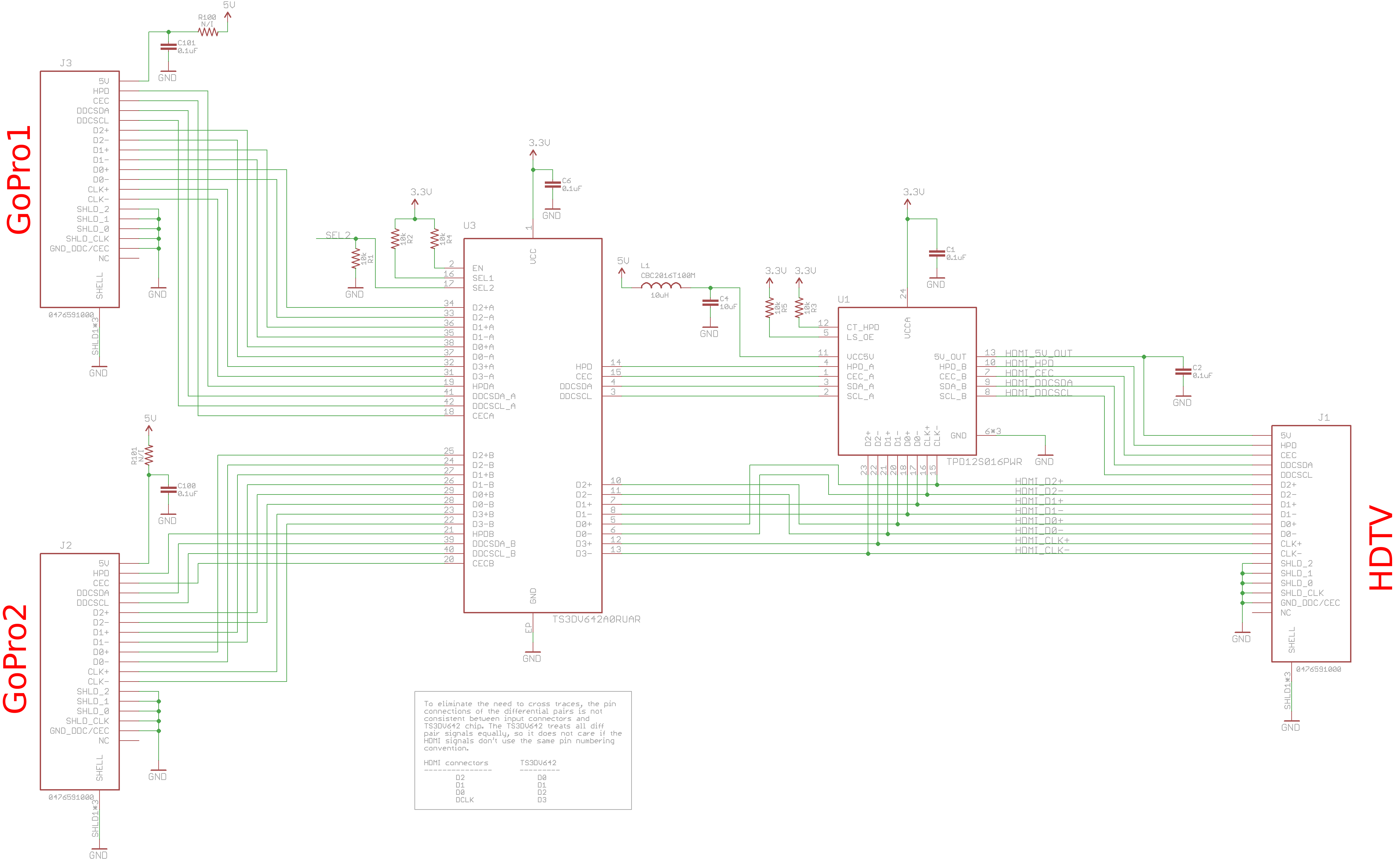
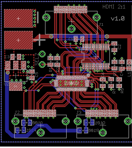
Here's my schematic and PCB layout for visual reference.
The left-most and right-most components in the schematic are the HDMI connectors (labeled "GoPro1", "GoPro2", and "HDTV"). Of the two IC's in the middle, the taller one is the 2:1 mux. The other one is a TPD12S016, which provides ESD protection and level shifting for the HDMI signal lines.
Since I don't have the right oscilloscope for the job right now, I'm focusing on the signals that I can see, namely, the HPD and I2C lines. I'm hoping someone that has a deep working understanding of the HDMI spec can point out an error in my design. Here's my considerations, troubleshooting steps I've taken so far, and questions:
1.I connected the GoPros I'm using directly into the HDTV to verify the HDMI cables are good and the display is compatible with the source. I've also tried several different kinds of HDMI displays and they all exhibit the same behavior.
2.I designed the schematic to have pull-up/down resistors on the SEL1/SEL2 pins of the mux so that it defaults to input A, which is "GoPro1" in my schematic.
3.I verified that the HPD pin of the GoPro1 connector goes high (~4V) when I plug in the HDTV connector and low when the HDTV is unplugged.
4.I verified the HDMI connectors on both sides have a steady 5V power source on the appropriate pin when everything is plugged in.
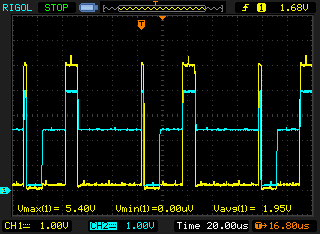
5.I initially found a weird problem with the SDA line of the DDC I2C port. At the HDTV connector side, the SDA signal looked good. Nice square waves that went from 0V to 5V. On the GoPro connector side, however, the signal achieved 3 different voltages: 0V, 2.5V, and 4V. The yellow line is the HDTV side and the blue line is the GoPro side.
It looks to me like a resistor divider is happening in there somehow. Since the TPD12S016 buffers the I2C lines, I suspected it was the problem. I lifted the relevant pin off the board and green-wired the SDA line directly between the GoPro1 and the HDTV connectors. Now the signal looks clean across the board. Can anyone suggest why it occasionally floated at 2.5V like that?
6.Is it correct to assume that an integrated consumer video device (like a GoPro) would take care of the pull-up resistors on the DDC I2C port?
7.I understand the DDC I2C port is used by the sink to tell the source about itself and vice versa. When I have a GoPro and the HDTV all connected, I see a continuous stream of I2C communication on the SDA line. Is it typical for the source and sink to continuously talk to each on the DDC port while connected? Or is that a sign that one of the devices is trying over and over to communicate but the other side isn't responding? I'm wondering if maybe the HDTV is waiting until successful DDC comms before it allows the video to be displayed.
8.Assuming the TMDS signals themselves are getting through (which I have no way of verifying right now), are there other common reasons that the HDMI sink will refuse to show the video stream?
Question
HDMI Switch Problems
This topic has been closed for further comments. You can use the search bar to find a similar topic, or create a new one by clicking Create Topic at the top of the page.
Enter your E-mail address. We'll send you an e-mail with instructions to reset your password.


